Thyristor
A thyristor using NPN and PNP transistors.
blockType: AcausalElectricPowerSystems.Semiconductors.Thyristor
|
Path in the library: |

Description
Block Thyristor allows you to model a thyristor in two ways:
-
In the form of an equivalent circuit based on NPN and PNP bipolar transistors.
-
Approximation of the I-V curve (current-voltage) in the switched-on state using the correspondence table.
Representation using an equivalent schema
The equivalent circuit contains a pair of NPN and PNP bipolar transistors, as shown in the following figure.
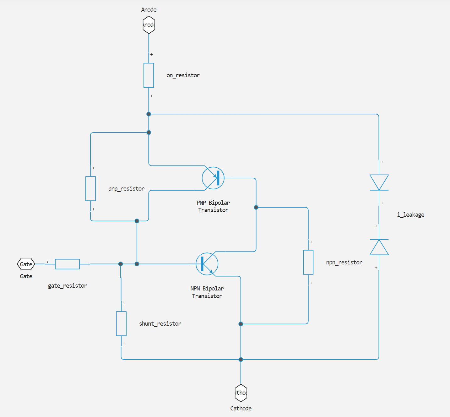
The structure of the P-N-P-N thyristor corresponds to the structures of P-N-P and N-P-N bipolar transistors, the base of each of which is connected to the collector of another device. In order for this circuit to behave like a thyristor, it is necessary to select the appropriate parameter values for NPN and PNP transistors, as well as external resistors. For example, in order for the circuit to be fixed in a conductive state after starting with the appropriate control current, the total gain of the two transistors must be greater than unity. This model structure reproduces the behavior of a thyristor in typical application circuits and at the same time presents the solver with a minimum number of equations, which increases the simulation speed.
| It is very important to properly parameterize the thyristor component before using it in your model. According to the technical data sheet of your device, change the parameters of the thyristor component so that it simulates the required behavior. Then you can copy the parameterized component to your model. Make sure to correctly model the connection diagram of the control electrode, including the series resistance of the circuit. Connecting a controlled voltage source directly to the control electrode of the thyristor gives non-physical results, since when the voltage on the control electrode is zero, it is pressed against the voltage on the cathode. |
The model reflects the following characteristics of the thyristor:
-
Currents in the closed state, and . They are usually specified for maximum voltages in the closed state. and . It is assumed, as for most thyristors, that and .
-
The release voltage at the control electrode is equal to Corresponding gate voltage, V_GT when the current in the control electrode is equal to the switching current of the thyristor, the value of the parameter Gate trigger current, I_GT.
-
The thyristor is switched on when the value of the control current reaches the value of the switching current of the thyristor., Gate trigger current, I_GT. The thyristor will not turn on until the control current reaches this value. To verify this, you must set the parameter correctly. Internal shunt resistor, Rs. If the resistance is too high, the thyristor will turn on before the control current reaches . If the resistance is too low, the thyristor will not turn on.
You can define the value Internal shunt resistor, Rs by running the simulation. If you use a thyristor in a circuit where there is an external resistor connected from the control electrode to the cathode, the effect of the resistance determined by the value of the parameter Internal shunt resistor, Rs it is usually very small, and it can be set to equal
Inf. -
If the thyristor is in the on state, then in the absence of a control signal, the thyristor remains in the on state, provided that the load current is greater than the holding current. The holding current is not set directly, as its value is mainly determined by other block parameters. However, the holding current can be affected by using the parameter Product of NPN and PNP forward current gains. Reducing the gain increases the holding current.
-
The switching voltage is equal to the voltage drop across the thyristor, the value of the parameter On-state voltage, V_T when the load current is equal to the switch-on current, the value of the parameter On-state current, I_T. This is provided by the resistance value , which takes into account the voltage drop across PNP and NPN devices.
-
Actuation by the rate of voltage rise in the closed state. A rapid change in the anode-cathode voltage causes a current in the base-collector circuit. If this current is large enough, it puts the thyristor in the open state. A suitable base-collector capacitance value is calculated so that at a voltage change rate equal to the maximum allowable voltage rise rate in the closed state, Critical rate of rise of off-state voltage, dV/dt the thyristor was triggered. This calculation is based on the approximation that the required current is , where – the resistance value between the control electrode and the cathode used in calculating the maximum allowable value Critical rate of rise of off-state voltage, dV/dt.
-
The power-on delay time mainly depends on the parameter value. NPN device forward transit time. You either specify this parameter directly, or calculate an approximate value. by the turn-on time.
-
The shutdown delay time, which is primarily affected by the parameter value PNP device forward transit time. You can set this parameter directly or set it to the forward travel time for the NPN transistor.
-
pnp_resistor and npn_resistor resistors increase the stability of the numerical solution at high forward and reverse voltages. Their values affect the shutdown currents by no more than 1% at the maximum voltages of the forward and reverse closed states.
| Since this implementation of the block includes a charge model, in order to obtain a clear dynamics of switching on and off the thyristor, it is necessary to simulate the total resistance of the circuit driving the gate. Therefore, if you simplify the control circuit of an electrode by presenting it as a controlled voltage source, you must turn on a suitable resistor in series between the voltage source and the control electrode. |
Parameterization using the correspondence table
When parameterizing a thyristor using a matching table, the value of the anode-cathode current is a function of the voltage between the anode and the cathode in the open state. The main advantages of using this option are the speed of modeling and ease of parameterization. To further simplify the basic model, this representation does not model:
-
Turning on the device due to the rate of voltage rise in the off state.
-
Shutdown delay time.
The switch-on delay is represented by an input capacitor between the control electrode and the cathode, the value of which is calculated so that the delay between the voltage rise on the control electrode and the start of switching on the device is equal to the value set by the parameter Turn-on delay time. The rise time of the load current when switched on is realized by a nonlinear increase in current from zero to the current determined by the current-voltage profile in the open state, over the time specified by the parameter value Turn-on rise time. Please note that the resulting switch-on current profile is an approximation to the actual device.
Modeling of thermal effects
A thermal port can be used to simulate the effect of the generated heat and the temperature of the device.:
If the check box Enable thermal port If not installed, the unit does not contain a heat port and does not simulate heat generation in the device. If the check box Enable thermal port If installed, the unit contains a thermal port that allows you to simulate heat generation due to heat loss. To ensure numerical efficiency, the thermal condition does not affect the electrical behavior of the unit.
Assumptions and limitations
-
Temperature-dependent effects are not modeled in this block. This block is modeled at the temperature specified in the parameter Measurement temperature. All parameters must be specified for this temperature.
-
If you are using an equivalent circuit model:
-
In circuits with a sensitive control electrode (that is, where there is no external resistor for the control electrode-cathode) it is necessary to set the value of the parameter Internal shunt resistor, Rs to ensure proper operation. If the internal resistance of the shunt is too high, then the thyristor is triggered at a current lower than . If the internal resistance of the shunt is too low, the thyristor will not operate at the input current. .
-
Operation when the breakdown voltage is exceeded is not simulated.
-
Numerical simulation of a thyristor can be difficult, given the very small control currents compared to the load current, as well as abrupt current changes during switching. However, for most typical thyristor-based circuits, the default simulation parameters can be used. In some cases, it may be necessary to adjust the parameters to ensure convergence. Absolute tolerance and Relative tolerance in the block Solver Configuration. In such cases, it is usually sufficient to change the default value. Absolute tolerance on
1e-4or1e-5because this prevents adaptive change of this parameter during simulation. -
The leakage currents are approximated by i-leakage diodes, as shown in the equivalent circuit. This approach assumes that the leakage through the two transistors is small in comparison. This assumption is not valid for values which are significantly less than the typical forward voltage drop
0.6V.
-
-
If you use a representation in the form of a matching table:
-
Triggering by exceeding the breakdown voltage or by the rate of voltage change in the off state is not simulated.
-
The shutdown delay time is not simulated. Check whether the circuit does not violate the set shutdown delay time.
-
When you specify the rise time of the on current, the resulting time dependence of the current is approximate.
-
Variables
Use the parameter group Initial Targets to set the priority and initial target values for the block parameter variables before modeling. For more information, see Configuring physical blocks using target values.
Ports
Conserving
#
A
—
The anode
electricity
Details
The electrical port connected to the anode.
| Program usage name |
|
#
K
—
The cathode
electricity
Details
The electrical port connected to the cathode.
| Program usage name |
|
#
G
—
control electrode
electricity
Details
The electrical port connected to the control electrode.
| Program usage name |
|
#
H
—
thermal port
warmth
Details
The thermal port.
Dependencies
To use this port, check the box Enable thermal port.
| Program usage name |
|
Parameters
Thermal Port
#
Thermal resistances, [R1, R2, ..., Rn] —
the vector of thermal resistances for the Kauer model
K/W
Details
Vector from the values of the thermal resistances represented by the Kauer elements in the heating network. All these values must be greater than zero.
Dependencies
To use this parameter, set for the parameter Thermal network meaning Cauer model.
| Units |
|
| Default value |
|
| Program usage name |
|
| Evaluatable |
Yes |
#
Thermal resistances, [R1, R2, ..., Rn] —
the vector of thermal resistances for the Foster model
K/W
Details
Vector from the values of thermal resistances represented by the coefficients of the Foster model in the heating network. All these values must be greater than zero.
Dependencies
To use this parameter, set for the parameter Thermal network meaning Cauer model parameterized with Foster coefficients.
| Units |
|
| Default value |
|
| Program usage name |
|
| Evaluatable |
Yes |
#
Thermal masses, [M1, M2, ..., Mn] —
vector of heat capacity values for the Kauer model
J/K | kJ/K
Details
Vector from values of heat capacities, where this is the number of coefficients of the Kauer model in the heat network. All these values must be greater than zero.
Dependencies
To use this parameter, set for the parameter Thermal network meaning Cauer model, and for the parameter Thermal mass parameterization meaning By thermal mass.
| Units |
|
| Default value |
|
| Program usage name |
|
| Evaluatable |
Yes |
#
Thermal masses, [M1, M2, ..., Mn] —
the vector of heat capacity values for the Foster model
J/K | kJ/K
Details
Vector from values of heat capacities, where this is the number of Foster elements in the heating network. All these values must be greater than zero.
Dependencies
To use this parameter, set for the parameter Thermal network meaning Cauer model parameterized with Foster coefficients, and for the parameter Thermal mass parameterization meaning By thermal mass.
| Units |
|
| Default value |
|
| Program usage name |
|
| Evaluatable |
Yes |
#
Thermal time constants, [t1, t2, ..., tn] —
vector of thermal time constants for the Kauer model
s | ns | us | ms | min | hr | d
Details
Vector from values of thermal time constants, where this is the number of Kauer elements in the heating network. All these values must be greater than zero.
The value of the heat capacity is calculated as , where , and — heat capacity, thermal time constant and thermal resistance for - the go element of the Cowera.
Dependencies
To use this parameter, set for the parameter Thermal network meaning Cauer model, and for the parameter Thermal mass parameterization meaning By thermal time constants.
| Units |
|
| Default value |
|
| Program usage name |
|
| Evaluatable |
Yes |
#
Thermal time constants, [t1, t2, ..., tn] —
the vector of thermal time constants for the Foster model
s | ns | us | ms | min | hr | d
Details
Vector from values of thermal time constants, where this is the number of coefficients of the Foster model in the heating network. All these values must be greater than zero.
The value of the heat capacity is calculated as , where , and — heat capacity, thermal time constant and thermal resistance for - the go element of the Cowera.
Dependencies
To use this parameter, set for the parameter Thermal network meaning Cauer model parameterized with Foster coefficients, and for the parameter Thermal mass parameterization meaning By thermal time constants.
| Units |
|
| Default value |
|
| Program usage name |
|
| Evaluatable |
Yes |
# Enable thermal port — turning on the heat port
Details
Select this option to use the thermal port of the unit and simulate the effect of the generated heat and the temperature of the device.
| Default value |
|
| Program usage name |
|
| Evaluatable |
No |
#
Thermal network —
choosing an internal thermal model
Specify junction and case thermal parameters | Cauer model | Cauer model parameterized with Foster coefficients | External
Details
Choose an internal thermal model:
-
Specify junction and case thermal parameters; -
Cauer model; -
Cauer model parameterized with Foster coefficients; -
External.
| Values |
|
| Default value |
|
| Program usage name |
|
| Evaluatable |
No |
#
Junction-case and case-ambient (or case-heatsink) thermal resistances, [R_JC, R_CA] —
the vector of thermal resistances
K/W
Details
Vector [R_JC, R_CA] of the two values of thermal resistance. The first value R_JC — this is the thermal resistance between the junction and the housing. The second value, R_CA — this is the thermal resistance between the H port and the device body.
Dependencies
To use this parameter, set for the parameter Thermal network meaning Specify junction and case thermal parameters.
| Units |
|
| Default value |
|
| Program usage name |
|
| Evaluatable |
Yes |
#
Thermal mass parameterization —
parameterization of heat capacity
By thermal time constants | By thermal mass
Details
Choose a method for setting the heat capacity:
-
By thermal time constants— parameterization of heat capacity in terms of thermal time constants. This value is used by default. -
By thermal mass— setting the heat capacity values.
Dependencies
To use this parameter, set for the parameter Thermal network meaning Specify junction and case thermal parameters, Cauer model or Cauer model parameterized with Foster coefficients.
| Values |
|
| Default value |
|
| Program usage name |
|
| Evaluatable |
No |
#
Junction and case thermal masses, [M_J, M_C] —
vector of heat capacity values for the Kauer model
J/K | kJ/K
Details
Vector [M_J, M_C] of the two values of the heat capacity. The first value M_J — this is the heat capacity of the transition. The second value, M_C — this is the heat capacity of the case.
Dependencies
To use this parameter, set for the parameter Thermal network meaning Specify junction and case thermal parameters, and for the parameter Thermal mass parameterization meaning By thermal mass.
| Units |
|
| Default value |
|
| Program usage name |
|
| Evaluatable |
Yes |
#
Junction and case thermal time constants, [t_J, t_C] —
vector of thermal time constants
s | ns | us | ms | min | hr | d
Details
Vector [t_J, t_C] of the two values of the thermal time constants. The first value t_J — this is the thermal transition time constant. The second value, t_C — this is the thermal time constant of the hull.
Dependencies
To use this parameter, set for the parameter Thermal network meaning Specify junction and case thermal parameters, and for the parameter Thermal mass parameterization meaning By thermal time constants.
| Units |
|
| Default value |
|
| Program usage name |
|
| Evaluatable |
Yes |
#
Junction and case initial temperatures, [T_J, T_C] —
vector of initial temperatures
K | degC | degF | degR | deltaK | deltadegC | deltadegF | deltadegR
Details
Vector [T_J, T_C] of the two temperature values. The first value T_J — this is the initial temperature of the transition. The second value, T_C — this is the initial temperature of the case.
Dependencies
To use this parameter, set for the parameter Thermal network meaning Specify junction and case thermal parameters.
| Units |
|
| Default value |
|
| Program usage name |
|
| Evaluatable |
Yes |
#
Thermal masses initial temperatures, [T1, T2, ..., Tn] —
initial temperature vector for the Kauer model
K | degC | degF | degR | deltaK | deltadegC | deltadegF | deltadegR
Details
The vector of temperature values. It corresponds to the temperature difference for each heat capacity in the model.
Dependencies
To use this parameter, set for the parameter Thermal network meaning Cauer model.
| Units |
|
| Default value |
|
| Program usage name |
|
| Evaluatable |
Yes |
#
Initial node temperatures, [T1, T2, ..., Tn] —
the initial temperature vector for the Foster model
K | degC | degF | degR | deltaK | deltadegC | deltadegF | deltadegR
Details
The vector of absolute temperature values of each element of the Foster model.
Dependencies
To use this parameter, set for the parameter Thermal network meaning Cauer model parameterized with Foster coefficients.
| Units |
|
| Default value |
|
| Program usage name |
|
| Evaluatable |
Yes |
Main
#
I-V characteristics defined by —
parameterization of the thyristor
Fundamental nonlinear equations | Lookup table
Details
Use a thyristor simulation or an equivalent circuit based on NPN and PNP bipolar transistors (Fundamental nonlinear equations), or an approximation of the I-V curve in the switched-on state using the table (Lookup table).
| Values |
|
| Default value |
|
| Program usage name |
|
| Evaluatable |
No |
#
On-state voltage, V_T —
voltage drop across the thyristor when switched on
V | uV | mV | kV | MV
Details
The static voltage drop of the anode-cathode in the switched-on state, while the flowing current is equal to the on current .
Dependencies
To use this parameter, set for the parameter I-V characteristics defined by meaning Fundamental nonlinear equations.
| Units |
|
| Default value |
|
| Program usage name |
|
| Evaluatable |
Yes |
#
On-state current, I_T —
static load current when switched on
A | pA | nA | uA | mA | kA | MA
Details
Static load current (anode current), which flows when the anode-cathode voltage is equal to the voltage in the enabled state.
Dependencies
To use this parameter, set for the parameter I-V characteristics defined by meaning Fundamental nonlinear equations.
| Units |
|
| Default value |
|
| Program usage name |
|
| Evaluatable |
Yes |
#
Vector of on-state voltages, V_T —
vector of voltage values in the open state
V | uV | mV | kV | MV
Details
The vector of voltage values in the open state, which will be used for searching in the table. The values of the vector must be strictly increasing, and the first value must be greater than zero. The values may be unevenly distributed.
Dependencies
To use this parameter, set for the parameter I-V characteristics defined by meaning Lookup table.
| Units |
|
| Default value |
|
| Program usage name |
|
| Evaluatable |
Yes |
#
Vector of corresponding currents, I_T —
the vector of values of the corresponding currents
A | pA | nA | uA | mA | kA | MA
Details
The vector of current values corresponding to the values of the switch-on voltage vector to be used for searching in the 1D table. These two vectors must be the same size.
Dependencies
To use this parameter, set for the parameter I-V characteristics defined by meaning Lookup table.
| Units |
|
| Default value |
|
| Program usage name |
|
| Evaluatable |
Yes |
#
Off-state current, I_DRM —
anode current in the off state
A | pA | nA | uA | mA | kA | MA
Details
Anode current in the off state , which occurs when the anode-cathode voltage is equal to the voltage in the off state .
| Units |
|
| Default value |
|
| Program usage name |
|
| Evaluatable |
Yes |
#
Corresponding off-state voltage, V_DRM —
anode-cathode voltage in the off state
V | uV | mV | kV | MV
Details
Anode-cathode voltage applied to the thyristor in the off state when the off state current is reached .
| Units |
|
| Default value |
|
| Program usage name |
|
| Evaluatable |
Yes |
#
Holding current —
holding current
A | pA | nA | uA | mA | kA | MA
Details
This is the minimum current at which the thyristor remains switched on. For the option Lookup table The latching current is assumed to be equal to the holding current, so it is also the maximum current at which the thyristor remains in the off state.
Dependencies
To use this parameter, set for the parameter I-V characteristics defined by meaning Lookup table.
| Units |
|
| Default value |
|
| Program usage name |
|
| Evaluatable |
Yes |
#
Measurement temperature —
Device simulation temperature
K | degC | degF | degR | deltaK | deltadegC | deltadegF | deltadegR
Details
The temperature of the device simulation. For this temperature, it is necessary to specify all the values of the block parameters.
Dependencies
To use this parameter, set for the parameter I-V characteristics defined by meaning Fundamental nonlinear equations.
| Units |
|
| Default value |
|
| Program usage name |
|
| Evaluatable |
Yes |
Gate triggering
#
Gate trigger current, I_GT —
switching current of the thyristor
A | pA | nA | uA | mA | kA | MA
Details
Threshold value of the current through the control electrode required to turn on the transistor, as a result of which the gate voltage becomes equal to the corresponding voltage on the control electrode . You must set the value of the parameter Internal shunt resistor, Rs to ensure that the shutter is triggered when , and not at currents lower than .
| Units |
|
| Default value |
|
| Program usage name |
|
| Evaluatable |
Yes |
#
Corresponding gate voltage, V_GT —
voltage between the control electrode and the cathode
V | uV | mV | kV | MV
Details
Voltage between the control electrode and the cathode when the current at the control electrode is equal to the switching current .
| Units |
|
| Default value |
|
| Program usage name |
|
| Evaluatable |
Yes |
#
Test voltage, V_D —
Test supply voltage
V | uV | mV | kV | MV
Details
The supply voltage used when specifying values and .
Dependencies
To use this parameter, set for the parameter I-V characteristics defined by meaning Fundamental nonlinear equations.
| Units |
|
| Default value |
|
| Program usage name |
|
| Evaluatable |
Yes |
#
Test load resistor —
test load resistor
Ohm | mOhm | kOhm | MOhm | GOhm
Details
The load resistor used in calculating the values and .
Dependencies
To use this parameter, set for the parameter I-V characteristics defined by meaning Fundamental nonlinear equations.
| Units |
|
| Default value |
|
| Program usage name |
|
| Evaluatable |
Yes |
dV/dt Triggering
#
Critical rate of rise of off-state voltage, dV/dt —
the maximum allowable rate of voltage rise in the off state
V/s | V/us
Details
If the voltage at the anode and cathode increases faster than this rate, the thyristor will experience a parasitic activation due to capacitive effects.
Dependencies
To use this parameter, set for the parameter I-V characteristics defined by meaning Fundamental nonlinear equations.
| Units |
|
| Default value |
|
| Program usage name |
|
| Evaluatable |
Yes |
#
Test gate-cathode resistor, R_GK —
test resistor between control electrode and cathode
Ohm | mOhm | kOhm | MOhm | GOhm
Details
A resistor between the control electrode and the cathode used in calculating the maximum allowable voltage rise rate in the off state.
Dependencies
To use this parameter, set for the parameter I-V characteristics defined by meaning Fundamental nonlinear equations.
| Units |
|
| Default value |
|
| Program usage name |
|
| Evaluatable |
Yes |
Time Constants
#
NPN device forward transit time parameterization —
parameterization of the forward running time of the NPN device
Derive approximate value from gate-controlled turn-on time | Specify directly
Details
Choose one of the following options:
-
Derive approximate value from gate-controlled turn-on time— the unit calculates the forward running time of the NPN device based on the switch-on time values you set and the corresponding control current. -
Specify directly— specify the value directly using the parameter NPN device forward transit time.
Dependencies
To use this parameter, set for the parameter I-V characteristics defined by meaning Fundamental nonlinear equations.
| Values |
|
| Default value |
|
| Program usage name |
|
| Evaluatable |
No |
#
Gate-controlled turn-on time —
delay time for switching on the thyristor after applying the control pulse
s | ns | us | ms | min | hr | d
Details
The time of the thyristor transition from the off state to the on state when the control current is applied.
| Units |
|
| Default value |
|
| Program usage name |
|
| Evaluatable |
Yes |
#
Corresponding gate current —
test current of the control electrode
A | pA | nA | uA | mA | kA | MA
Details
The current on the control electrode used to determine the delay time for switching on the thyristor after applying the control pulse. The gate current and the switch-on time are used to calculate the approximate forward travel time of the NPN device, assuming that the entire input charge is used to boost the gate voltage to the corresponding gate voltage. . The default value is 10 mA.
Dependencies
To use this parameter, set for the parameter I-V characteristics defined by meaning Fundamental nonlinear equations, and for the parameter NPN device forward transit time parameterization meaning Derive approximate value from gate-controlled turn-on time.
| Units |
|
| Default value |
|
| Program usage name |
|
| Evaluatable |
Yes |
#
NPN device forward transit time —
average forward passage time
s | ns | us | ms | min | hr | d
Details
The average transit time of non-primary charge carriers through the base region from the emitter to the collector of the NPN device [1].
Dependencies
To use this parameter, set for the parameter I-V characteristics defined by meaning Fundamental nonlinear equations, and for the parameter NPN device forward transit time parameterization meaning Derive approximate value from gate-controlled turn-on time.
| Units |
|
| Default value |
|
| Program usage name |
|
| Evaluatable |
Yes |
#
PNP device forward transit time parameterization —
parameterization of the direct transit time of the PNP device
Set equal to NPN device forward transit time | Specify directly
Details
Choose one of the following options:
-
Set equal to NPN device forward transit time— the block uses the time value of the direct transit of the NPN device. -
Specify directly— specify the value directly using the time parameter PNP device forward transit time.
Dependencies
To use this parameter, set for the parameter I-V characteristics defined by meaning Fundamental nonlinear equations.
| Values |
|
| Default value |
|
| Program usage name |
|
| Evaluatable |
No |
#
PNP device forward transit time —
average forward passage time
s | ns | us | ms | min | hr | d
Details
The average transit time of non-primary charge carriers through the base region from the emitter to the collector of the PNP device [1].
Dependencies
To use this parameter, set for the parameter I-V characteristics defined by meaning Fundamental nonlinear equations, and for the parameter PNP device forward transit time parameterization meaning Set equal to NPN device forward transit time .
| Units |
|
| Default value |
|
| Program usage name |
|
| Evaluatable |
Yes |
#
Turn-on delay time —
delay time for switching on the thyristor
s | ns | us | ms | min | hr | d
Details
The delay time for switching on the thyristor after changing the current on the control electrode from zero to the value set by the parameter Gate current for turn-on delay time.
Dependencies
To use this parameter, set for the parameter I-V characteristics defined by meaning Lookup table.
| Units |
|
| Default value |
|
| Program usage name |
|
| Evaluatable |
Yes |
#
Gate current for turn-on delay time —
current at the control electrode for the switch-on delay time
A | pA | nA | uA | mA | kA | MA
Details
The current at the control electrode used to measure the switch-on delay time.
Dependencies
To use this parameter, set for the parameter I-V characteristics defined by meaning Lookup table.
| Units |
|
| Default value |
|
| Program usage name |
|
| Evaluatable |
Yes |
#
Turn-on rise time —
the rise time of the on signal
s | ns | us | ms | min | hr | d
Details
The time it takes for the thyristor to fully turn on after the power-on delay time has passed.
Dependencies
To use this parameter, set for the parameter I-V characteristics defined by meaning Lookup table.
| Units |
|
| Default value |
|
| Program usage name |
|
| Evaluatable |
Yes |
Advanced
#
Internal shunt resistor, Rs —
shunt resistance between the control electrode and the cathode
Ohm | mOhm | kOhm | MOhm | GOhm
Details
The resistance of the shunt between the control electrode and the cathode. It is important to set the value of this parameter so that the shutter is triggered when , and not at currents lower than . If you use a thyristor in a circuit where there is an external resistor , then usually the impact it is small, and it can be set to equal Inf.
Dependencies
To use this parameter, set for the parameter I-V characteristics defined by meaning Fundamental nonlinear equations.
| Units |
|
| Default value |
|
| Program usage name |
|
| Evaluatable |
Yes |
#
Internal series gate resistor, Rg —
the resistance associated with the connection of the control electrode
Ohm | mOhm | kOhm | MOhm | GOhm
Details
The resistance associated with the connection of the control electrode. A typical value is on the order of a few ohms, and its effect on static and dynamic characteristics is small. Therefore, its exact value is not so important, but its presence helps to avoid problems in numerical simulation if the gate is controlled directly by a voltage source. You can specify any positive value.
| Units |
|
| Default value |
|
| Program usage name |
|
| Evaluatable |
Yes |
# Product of NPN and PNP forward current gains — the product of the forward current gain coefficients NPN and PNP
Details
This is the product of the NPN forward current gain and the forward current gain PNP . The value must be greater than one for the fixation to occur. The lower the value, the greater the locking current. However, the locking current is mainly set by other block parameters, and the overall gain has only a minor effect.
Dependencies
To use this parameter, set for the parameter I-V characteristics defined by meaning Fundamental nonlinear equations.
| Default value |
|
| Program usage name |
|
| Evaluatable |
Yes |