Technical description of the hardware
RF switches
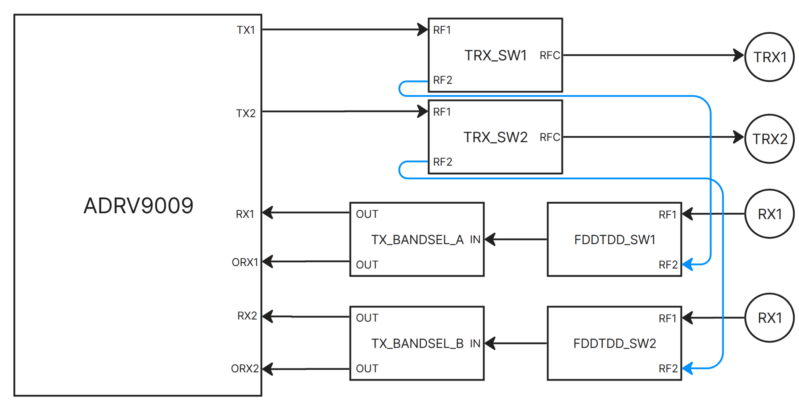
With the help of radio frequency switches located in the RITM of the SDR USRP, it is possible to switch the signal from the output of the transceiver ADRV9009 to the external connectors of the device, or to the internal RF loop back to the receiving part. The block diagram of RF switches is shown in the figure.
Interfaces and connectors
Radio frequency connectors
-
TRX1 — transmitter output, first channel;
-
TRX2 — transmitter output, second channel;
-
RX1 — receiver input, first channel;
-
RX2 — receiver input, second channel;
-
REF IN — reference clock input (10 or 48 MHz);
-
REF OUT — output of the reference clock signal (48 MHz).
Interfaces
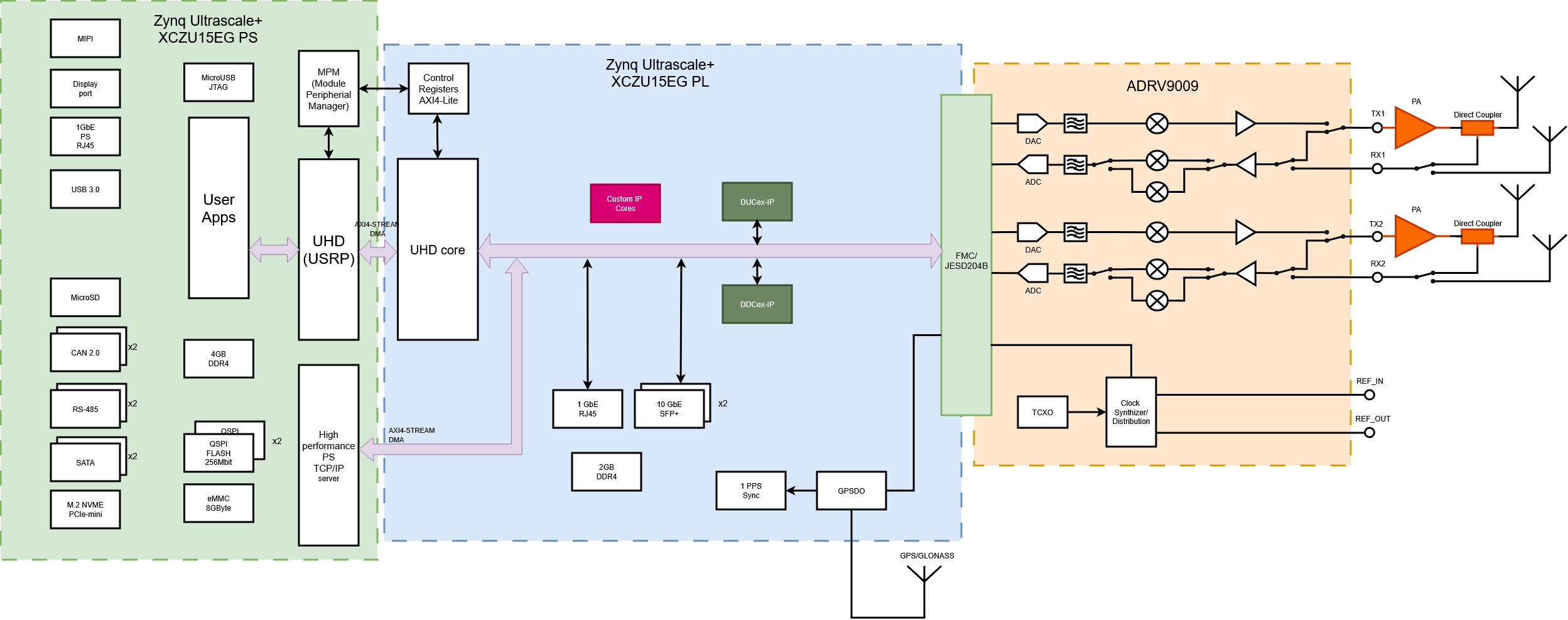
RITM SDR USRP supports many different interfaces:
-
USB 3.0;
-
PS ethernet RJ45 1G;
-
PL ethernet RJ45;
-
PL SFP+ ethernet 10G;
-
M.2 NVME;
-
MIPI;
-
DisplayPort;
-
CAN 2.0;
-
RS-485 ;
-
SATA.
Synchronization with external signals and GPSDO
Thanks to the presence of the GPSDO module, it is possible to work with synchronized signals. By default, the PLL, which clocks the PL blocks associated with JESD, works in the mode holdover, i.e. without synchronization by an external reference signal. For synchronization with external devices, a mode is provided in which a reference signal of 10 or 48 MHz is applied to the input REF IN, the PLL exits the mode holdover and it synchronizes the phase of the output clock signal by the input.
Also, the RITM SDR USRP provides a REF OUT output of the reference synchronized frequency of 48 MHz for synchronization of other devices.
Thus, synchronous operation of several devices using a reference clock signal is possible.