Boost Converter
Controller-controlled step-up DC-DC voltage regulator.
blockType: AcausalElectricPowerSystems.Converters.Boost
|
Path in the library: |

Description
Block Boost Converter It is a converter that increases the DC voltage under the control of a connected controller and a gate signal generator. Boost converters are also known as boost voltage regulators because they increase the amount of voltage.
Block Boost Converter allows you to simulate an asynchronous converter with one switching device or a synchronous converter with two switching devices. The following types of switching devices are possible:
-
GTO— lockable thyristor. For information about the volt-ampere characteristic (VAC) of the device, see GTO. -
Ideal Semiconductor Switch— Perfect semiconductor controlled switch. For information about the device’s specifications, see Ideal Semiconductor Switch. -
IGBT— An ideal insulated gate bipolar transistor for switching circuits. For information about the device’s specifications, see IGBT (Ideal, Switching). -
MOSFET— perfect -channel MOSFET for switching circuits. For information about the device’s specifications, see MOSFET (Ideal, Switching). -
Thyristor— a thyristor with a piecewise linear VAC. For information about the device’s specifications, see Thyristor (Piecewise Linear). -
Averaged Switch— an average converter. The control signal port G takes values in the range from0before1. When the value of G is0or1,Averaged Switchfully open or fully closed, respectively. The key behaves similarly to the block Ideal Semiconductor Switch with an antiparallel diode. When the value of G is between0before1,Averaged Switchpartially open. You can average the signal using a pulse width modulation unit (PWM) for a certain period of time. This allows you to perform model subsampling and use modulation signals instead of PWM signals.
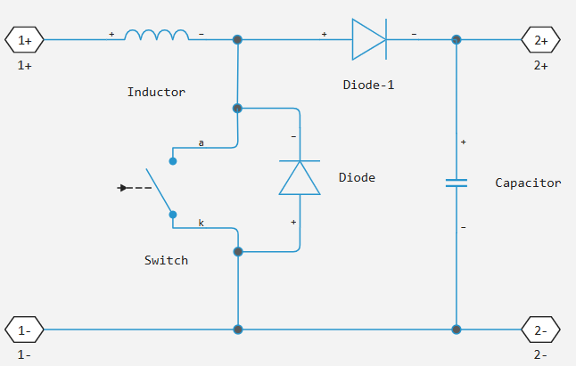
The topology of the converter
You can simulate Boost Converter as an asynchronous converter with a scalar gate control port or with two electrical control ports or as a synchronous converter with one electrical control port. To select the topology of the converter, set the parameter Modeling option meaning:
-
Nonsynchronous converter— asynchronous converter with additional scalar or electrical gate control ports; -
Synchronous converter— synchronous converter with multiplexed gate signals.
Asynchronous boost converter models contain an inductor, an electronic power switch, a diode, and an output capacitor.
The synchronous boost converter model contains an inductor, two electronic power switches and an output capacitor.
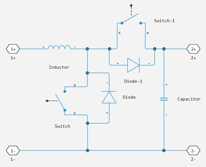
In each case, the capacitor smooths the output voltage.
Protection
You can include integrated protective diodes in the synchronous converter model. Integrated diodes protect a semiconductor device by providing a conductive path for reverse current. An inductive load can create a high reverse voltage surge when a semiconductor device suddenly cuts off the voltage supply to the load.
To enable and configure the internal protective diodes, use the parameters Diode.
This table shows how to set the parameter Model dynamics depending on your goals.
Goals |
Value for selection |
Built-in protective diode |
|
Do not turn on the protection |
|
Absent |
|
Turn on the protection |
Give priority to simulation speed. |
|
Block Diode |
The priority of the accuracy of the model is to accurately indicate the charge dynamics in the reverse mode. |
|
Dynamic block model Diode |
|
You can also include a snubber circuit for each switching device. Snubber circuits contain a series-connected resistor and capacitor. They protect switching devices from the high voltage that inductive loads create when the device turns off the voltage supply to the load. In addition, snubber circuits prevent excessive current change rates when switching on the switching device.
To enable and configure the snubber circuit for each switching device, use the parameters Snubbers.
Connecting signals to the gate control port
-
Asynchronous converter model (
Nonsynchronous converter) with directional control port option (Signal control port):-
Create a directional control signal, for example, from basic mathematical blocks, and connect it to the G port.
-
-
Asynchronous converter model (
Nonsynchronous converter) with the option of an electric control port (Electrical control port):-
Connect a positive DC voltage signal to the G+ port;
-
Connect the negative DC voltage signal to the G- port.
-
-
Synchronous converter model (
Synchronous converter):-
Multiplex the converted gate control signals into a single vector using a two-pulse gate multiplexer (see Two-Pulse Gate Multiplexer);
-
Connect the vector signal to the G port.
-
Piecewise constant approximation in an averaged commutator
If set for the parameter Switching device meaning Averaged Switch and use the partitioning solver, block, to create the model. Boost Converter creates nonlinear splits because the equations of the averaged mode include modes , which are functions of the input signal G. To activate the piecewise constant approximation, set the parameter Integer for piecewise constant approximation of gate input (0 for disabled) a value greater than 0. Then this block will consider the mode as a piecewise constant integer with a fixed range. This transforms previously non-linear partitions into linear, time-varying ones.
An integer value in the range [0, K], where — parameter value Integer for piecewise constant approximation of gate input (0 for disabled), is now associated with each mode of the real value in the range [0, 1]. The block calculates the piecewise constant approximation mode by dividing the initial mode by to normalize it back to the range [0, 1]:
Ports
Conserving
#
2+
—
positive output terminal
scalar
Details
An electrical port connected to the positive terminal 2 of the DC voltage.
| Program usage name |
|
#
2–
—
negative output terminal
scalar
Details
An electrical port connected to the negative terminal 2 of the DC voltage.
| Program usage name |
|
#
1+
—
positive input terminal
scalar
Details
The electrical port connected to the positive terminal 1 of the DC voltage.
| Program usage name |
|
#
1–
—
negative input terminal
scalar
Details
The electrical port connected to the negative terminal 1 of the DC voltage.
| Program usage name |
|
#
G+
—
the positive terminal of the switching device
electricity
Details
The electrical port connected to the positive gate terminal of the switching device.
Dependencies
To enable this port, set the parameter Modeling option meaning Nonsynchronous converter and for the parameter Gate-control port meaning Electrical.
| Program usage name |
|
#
G–
—
the negative terminal of the switching device
electricity
Details
The electrical port connected to the negative gate terminal of the switching device.
Dependencies
To enable this port, set the parameter Modeling option meaning Nonsynchronous converter and for the parameter Gate-control port meaning Electrical.
| Program usage name |
|
#
G
—
shutter contact
electricity
Details
The electrical port connected to the gate contact of the switch.
Dependencies
To enable this port, set the parameter Modeling option meaning Synchronous converter.
| Program usage name |
|
Input
#
G
—
shutter contact
scalar
Details
The control signal port connected to the switch gate.
Dependencies
To enable this port, set the parameter Modeling option meaning Nonsynchronous converter and for the parameter Gate-control port meaning Signal.
| Data types |
|
| Complex numbers support |
No |
Parameters
Main
#
Modeling option —
simulation of asynchronous or synchronous converter
Nonsynchronous converter | Synchronous converter
Details
Selecting the asynchronous or synchronous converter model.
| Values |
|
| Default value |
|
| Program usage name |
|
| Evaluatable |
No |
Switching device
#
Gate-control port —
defines the control port: scalar or electric
Signal | Electrical
Details
Scalar or electric gate control port of the switch.
Dependencies
To enable this port, set the parameter Modeling option meaning Nonsynchronous converter.
| Values |
|
| Default value |
|
| Program usage name |
|
| Evaluatable |
No |
#
Switching device —
switch type
GTO | Ideal Semiconductor Switch | IGBT | MOSFET | Thyristor | Averaged Switch
Details
The type of switching device for the converter. The switches are identical for the synchronous model.
| Values |
|
| Default value |
|
| Program usage name |
|
| Evaluatable |
No |
#
Forward voltage —
The direct current voltage of the switch
V | uV | mV | kV | MV
Details
For different types of switching devices, the parameter Forward voltage calculated as follows:
-
For
GTO— the minimum voltage required at the ports of the anode and cathode blocks so that the slope of the volt-ampere characteristic (VAC) of the device is , where — parameter value On-state resistance; -
For
IGBT— the minimum voltage required at the collector and emitter ports so that the slope of the VAX diode is , where — parameter value On-state resistance; -
For
Thyristor— the minimum voltage required to turn on the device.
Dependencies
To use this parameter, set for the parameter Switching device meaning GTO, IGBT or Thyristor .
| Units |
|
| Default value |
|
| Program usage name |
|
| Evaluatable |
Yes |
#
On-state resistance —
the resistance of the switch in the switched-on state
Ohm | mOhm | kOhm | MOhm | GOhm
Details
The resistance between the anode and the cathode when switched on.
For different types of switching devices, the parameter On-state resistance calculated as follows:
-
For
GTO— the rate of voltage change relative to the current is higher than the forward voltage; -
For
Ideal Semiconductor Switch— anode-cathode resistance when the device is switched on; -
For
IGBT— collector-emitter resistance when the device is switched on; -
For
Thyristor— anode-cathode resistance when the device is switched on; -
For
Averaged Switch— anode-cathode resistance when the device is switched on.
| Units |
|
| Default value |
|
| Program usage name |
|
| Evaluatable |
Yes |
#
Drain-source on resistance —
open channel MOSFET resistance
Ohm | mOhm | kOhm | MOhm | GOhm
Details
The resistance between the drain and the source, which also depends on the voltage between the gate and the source.
Dependencies
To use this parameter, set for the parameter Switching device meaning MOSFET.
| Units |
|
| Default value |
|
| Program usage name |
|
| Evaluatable |
Yes |
#
Off-state conductance —
the conductivity of the switch in the off state
S | nS | uS | mS | 1/Ohm
Details
The anode-cathode conductivity is switched off. The value should be less than , where — parameter value On-state resistance. For different types of switching devices, the resistance at rest is calculated as follows:
-
For
GTO— anode-cathode conductivity; -
For
Ideal Semiconductor Switch— anode-cathode conductivity; -
For
IGBT— collector-emitter conductivity; -
For
MOSFET— drain-source conductivity; -
For
Thyristor— anode-cathode conductivity.
Dependencies
To use this parameter, set for the parameter Switching device meaning GTO, Ideal Semiconductor Switch, IGBT, MOSFET or Thyristor.
| Units |
|
| Default value |
|
| Program usage name |
|
| Evaluatable |
Yes |
#
Threshold voltage —
switch threshold voltage
V | uV | mV | kV | MV
Details
The threshold voltage for the gate-cathode circuit. The switch turns on when the gate-cathode circuit voltage exceeds this value. For different types of switching devices, the parameter Threshold voltage calculated as follows:
-
For
Ideal Semiconductor Switch— gate-cathode voltage; -
For
IGBT— gate-emitter voltage; -
For
MOSFET— gate-source voltage.
Dependencies
To use this parameter, set for the parameter Switching device meaning Ideal Semiconductor Switch, IGBT or MOSFET.
| Units |
|
| Default value |
|
| Program usage name |
|
| Evaluatable |
Yes |
#
Gate trigger voltage —
switch threshold voltage
V | uV | mV | kV | MV
Details
The threshold voltage for the gate-cathode circuit. The device turns on when the gate-cathode circuit voltage exceeds this value.
Dependencies
To use this parameter, set for the parameter Switching device meaning GTO or Thyristor.
| Units |
|
| Default value |
|
| Program usage name |
|
| Evaluatable |
Yes |
#
Gate turn-off voltage —
switch threshold voltage
V | uV | mV | kV | MV
Details
The threshold voltage for the gate-cathode circuit. The device turns off when the gate-cathode circuit voltage drops below this value.
Dependencies
To use this parameter, set for the parameter Switching device meaning GTO or Thyristor.
| Units |
|
| Default value |
|
| Program usage name |
|
| Evaluatable |
Yes |
#
Holding current —
switch threshold current
A | pA | nA | uA | mA | kA | MA
Details
Threshold gate current. The device remains switched on when the current exceeds this value, even when the voltage between the gate and the cathode drops below the gate actuation voltage.
Dependencies
To use this parameter, set for the parameter Switching device meaning GTO or Thyristor.
| Units |
|
| Default value |
|
| Program usage name |
|
| Evaluatable |
Yes |
# Integer for piecewise constant approximation of gate input (0 for disabled) — piecewise constant approximation
Details
An integer used to perform a piecewise constant approximation of the gate input data.
Dependencies
To use this parameter, set for the parameter Switching device meaning Averaged Switch.
| Default value |
|
| Program usage name |
|
| Evaluatable |
Yes |
Diode
#
Model dynamics —
internal protective diode (suppressor) for synchronous topology
None | Diode with no dynamics | Diode with charge dynamics
Details
Specify whether the unit includes a protective diode (suppressor).
The following options are possible:
-
None— do not use a diode; -
Diode with no dynamics— select this option to prioritize the simulation speed using the block Diode. This option is used by default for asynchronous converter; -
Diode with charge dynamics— Select this option to increase the accuracy of the model in terms of charge dynamics in reverse mode using the switching diode model of the block Diode.
If for the parameter Switching device the value is selected in the settings Averaged Switch, this parameter is not displayed, and for the parameter Model dynamics The value is set automatically Diode with no dynamics.
|
Dependencies
To use this parameter, set for the parameter Modeling option meaning Synchronous converter.
| Values |
|
| Default value |
|
| Program usage name |
|
| Evaluatable |
No |
#
Model dynamics —
internal protective diode (suppressor) for asynchronous topology
Diode with no dynamics | Diode with charge dynamics
Details
The type of diode.
The following options are possible:
-
Diode with no dynamics— select this option to prioritize the simulation speed using the block Diode. This option is used by default for asynchronous converter; -
Diode with charge dynamics— Select this option to increase the accuracy of the model in terms of charge dynamics in reverse mode using the switching diode block model. Diode.
Dependencies
To use this parameter, set for the parameter Modeling option meaning Nonsynchronous converter.
| Values |
|
| Default value |
|
| Program usage name |
|
| Evaluatable |
No |
#
Forward voltage —
forward current voltage of the diode
V | uV | mV | kV | MV
Details
The minimum voltage required by the + and − ports of the unit in order for the gradient of the volt-ampere characteristic of the diode to be equal to , where — the resistance value on the switched switch.
Dependencies
To use this parameter, set for the parameter Model dynamics meaning Diode with no dynamics or Diode with charge dynamics.
| Units |
|
| Default value |
|
| Program usage name |
|
| Evaluatable |
Yes |
#
On resistance —
diode resistance when switched on directly
Ohm | mOhm | kOhm | MOhm | GOhm
Details
The resistance of the diode in the open state.
Dependencies
To use this parameter, set for the parameter Model dynamics meaning Diode with no dynamics or Diode with charge dynamics.
| Units |
|
| Default value |
|
| Program usage name |
|
| Evaluatable |
Yes |
#
Off conductance —
the conductivity of the diode in the closed state
S | nS | uS | mS | 1/Ohm
Details
The conductivity of the diode when it is switched back on.
Dependencies
To use this parameter, set for the parameter Model dynamics meaning Diode with no dynamics or Diode with charge dynamics.
| Units |
|
| Default value |
|
| Program usage name |
|
| Evaluatable |
Yes |
#
Junction capacitance —
diode junction capacity
F | pF | nF | uF | mF
Details
The value of the capacitance characteristic of the transition from the depleted zone, acting as a dielectric and separating the connections of the anode and cathode.
Dependencies
To use this parameter, set for the parameter Model dynamics meaning Diode with charge dynamics.
| Units |
|
| Default value |
|
| Program usage name |
|
| Evaluatable |
Yes |
#
Peak reverse current, iRM —
peak reverse current of the diode
A | pA | nA | uA | mA | kA | MA
Details
The peak return current measured by the external test circuit. This value must be less than zero.
Dependencies
To use this parameter, set for the parameter Model dynamics meaning Diode with charge dynamics.
| Units |
|
| Default value |
|
| Program usage name |
|
| Evaluatable |
Yes |
#
Initial forward current when measuring iRM —
the initial forward current of the diode during iRM measurement
A | pA | nA | uA | mA | kA | MA
Details
The initial forward current (at the initial moment of the switch-on time) when measuring the peak reverse current. This value must be greater than zero.
Dependencies
To use this parameter, set for the parameter Model dynamics meaning Diode with charge dynamics.
| Units |
|
| Default value |
|
| Program usage name |
|
| Evaluatable |
Yes |
#
Rate of change of current when measuring iRM —
the rate of change of diode current during iRM measurement
A/s | A/us
Details
The rate of change of the current when measuring the peak reverse current. This value must be less than zero.
Dependencies
To use this parameter, set for the parameter Model dynamics meaning Diode with charge dynamics.
| Units |
|
| Default value |
|
| Program usage name |
|
| Evaluatable |
Yes |
#
Reverse recovery time parameterization —
method for determining the reverse recovery time of a diode
Specify stretch factor | Specify reverse recovery time directly | Specify reverse recovery charge
Details
Defines the method for setting the reverse recovery time in the block.
When selecting an option Specify stretch factor or Specify reverse recovery charge the value that is used by the block to calculate the reverse recovery time is specified.
Dependencies
To use this parameter, set for the parameter Model dynamics meaning Diode with charge dynamics.
| Values |
|
| Default value |
|
| Program usage name |
|
| Evaluatable |
No |
# Reverse recovery time stretch factor — The stretching coefficient of the reverse recovery time of the diode
Details
The value that the block uses for calculation Reverse recovery time, trr. This value should be higher. 1. Specifying the stretching coefficient is an easier way to parameterize the reverse recovery time than specifying the reverse recovery charge. The higher the value of the stretching coefficient, the longer it takes for the reverse recovery current to dissipate.
Dependencies
To use this parameter, set for the parameter Model dynamics meaning Diode with charge dynamics, and for the parameter Reverse recovery time parameterization meaning Specify stretch factor.
| Default value |
|
| Program usage name |
|
| Evaluatable |
Yes |
#
Reverse recovery time, trr —
reverse diode recovery time
s | ns | us | ms | min | hr | d
Details
The amount of time it takes for a diode to turn off when the voltage across it reverses from forward bias to reverse.
The interval between the moment of the initial transition of the current through zero (when the diode turns off) and the moment the current drops to a level less than 10% of the peak current. Parameter Value Reverse recovery time, trr there must be more than the parameter value. Peak reverse current, iRM, divided by the parameter value Rate of change of current when measuring iRM.
The interval between the moment when the current initially becomes zero (when the diode turns off) and the moment when the current drops to less than 10% of the peak return current.
Dependencies
To use this parameter, set for the parameter Model dynamics meaning Diode with charge dynamics, and for the parameter Reverse recovery time parameterization meaning Specify reverse recovery time directly.
| Units |
|
| Default value |
|
| Program usage name |
|
| Evaluatable |
Yes |
#
Reverse recovery charge, Qrr —
reverse diode recovery charge
C | nC | uC | mC | nA*s | uA*s | mA*s | A*s | mA*hr | A*hr | kA*hr | MA*hr
Details
The value that the block uses for calculation Reverse recovery time, trr. Use this parameter if the reverse recovery charge value is specified in the block parameters as the type of reverse recovery time determination instead of the reverse recovery time value.
The reverse recovery charge is the total charge that continues to dissipate after the diode is turned off. The value must be less than , where
-
— the value specified for the parameter Peak reverse current, iRM;
-
— the value specified for the parameter Rate of change of current when measuring iRM.
| Units |
|
| Default value |
|
| Program usage name |
|
| Evaluatable |
Yes |
LC parameters
#
Inductance —
internal inductance
H | nH | uH | mH
Details
The inductance.
| Units |
|
| Default value |
|
| Program usage name |
|
| Evaluatable |
Yes |
#
Inductance series resistance —
series resistance of the inductor
Ohm | mOhm | kOhm | MOhm | GOhm
Details
The series resistance of the inductor.
| Units |
|
| Default value |
|
| Program usage name |
|
| Evaluatable |
Yes |
#
Capacitance —
internal capacity
F | pF | nF | uF | mF
Details
Container.
| Units |
|
| Default value |
|
| Program usage name |
|
| Evaluatable |
Yes |
#
Capacitor effective series resistance —
capacitor resistance
Ohm | mOhm | kOhm | MOhm | GOhm
Details
The series resistance of the capacitor.
| Units |
|
| Default value |
|
| Program usage name |
|
| Evaluatable |
Yes |
Snubbers
# Snubber — activating the damper
Details
Adding a damper to the switching device.
| Default value |
|
| Program usage name |
|
| Evaluatable |
No |
#
Snubber capacitance —
damper capacity
F | pF | nF | uF | mF
Details
The capacity of the switching device damper.
Dependencies
To use this option, check the box for the option Snubber.
| Units |
|
| Default value |
|
| Program usage name |
|
| Evaluatable |
Yes |
#
Snubber resistance —
damper resistance
Ohm | mOhm | kOhm | MOhm | GOhm
Details
The resistance of the switching device damper.
Dependencies
To use this option, check the box for the option Snubber.
| Units |
|
| Default value |
|
| Program usage name |
|
| Evaluatable |
Yes |